During AMD’s Capsacin event, held during GDC 2016, the company revealed their upcoming roadmap of graphics cards for the upcoming years and we learned that following on from Polaris (which shall debut this year) AMD will be releasing their first HBM2 GPU, codenamed Vega.
A LinkedIn profile has hinted what we might expect to find inside of Vega (also known as Greenland). The profile, which belongs to Yu Zhend, the manager of R&D over at AMD, states as one of his accomplishments “as leading chip of the first graphic IP V9.0 generation, it has full capacity of 4096 shader processor, along with the whole new SOC V15 architecture.”
The sentence gives a lot of insight into the project – for a start, “leading chip” tells us that it will likely be the flagship GPU in the Vega lineup. And we know from official slides from AMD that Vega 10 will be the lineup which debuts High Bandwidth Memory 2. It’s thought one of the big reasons the GPU has been put back is because of the delays of HBM2 manufacturing, 4GB DRAM chips won’t release until Q3, and Q4 will see the introduction of 8GB.
You might take issue with the number of shaders the Vega / Greenland flagship packs into a 14nm FinFet process. The 28nm Fiji (AMD’s Radeon Fury X card which comes loaded with 4GB HBM1) also offers 4096 shaders – so what gives?
During AMD’s RTG Technology Summit held earlier this year, the company made mention of a few changes to the GPU which could help improve the performance and efficiency of the shaders.
For example, improvements to Memory Compression were highlighted. Tonga introduced improvements to compression as well, so it will be interesting how much further AMD can push this technology.

Primitive Discard Accelerator, Hardware Scheduler, Improved Shader Efficiency and Instruction Pre-Fetch were what AMD wanted to share with us. Reading over this list and it means that not only will the GPU’s Shader Cores be more efficient at processing instructions, but instructions will be scheduled across those cores faster and better than previous cores.
Remember that another leak a few days ago hinted that the GPU’s we’ve seen of Polaris (more specifically, Polaris 10) will have 2,304 shaders inside, but this is most certainly an engineering sample given the memory configuration and core clocks.
In theory, this will allow the 4th generation GPU’s (presumably starting with Polaris and getting a tweak or two for Vega) to be faster at the same clock speeds as we’re currently seeing with GPU’s such as the Radeon 300 series.
One thing we’ve yet to discuss in the article is Graphic IP V9, and and here’s where things get a little more interesting. The same Linked In Profile confirms this, mentioning Project Fiji (the Radeon R9 290) which is Graphic IP V8.0. If you need some evidence, AMD’s own website makes mention of fixes for IP V7 and V8 families of GPUs. A user over at PC Tuning Forums, Yuri.CS put together a handy table for reference (but doesn’t include Vega).
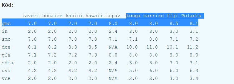
What all of this means is that Polaris is going to be more of a stepping stone, with larger changes to Vega 10 / Greenland. For reference:
GMC – Graphics Memory Controller
IH – Interrupt Handler
SMC– System Management Controller
DCE – Display Controller Engine
GFX – Graphics IP Revision
SDMA – System Direct Memory Access
UVD – Unified Video Decoder
VCE – Video Coding Engine
Of course, all of this isn’t confirmation from AMD of the specifications of Vega 10 (or Polaris for that matter). All we can do is wait for some official confirmation.
Source – 3D Center