AMD are back in the PR limelight, dominating much of the technology and gaming talk with their upcoming Zen architecture. Enthusiasts debate on the performance of the processor, speculate the price points (particularly when it comes to Summit Ridge, the Zen based platform for the desktop) and how their chips will stack up against Intel’s own lineup – particularly given Intel will likely have Kaby Lake to compete for the ‘mainstream’ crowd.
During Hot Chips 28, AMD decided to reveal even more information on the inner workings of the Zen CPU’s, delving much deeper into how they’ve achieved the touted “over 40% IPC gains” over their previous generation of processors, and more over; how they’re now neck and neck with one of Intel’s best: an I7-6900K.
During part 1 of our technical analysis, we looked at the processor from a broad overview, examining the improvements in caching, touched on Zen’s 14nm FinFet advancements and the basics of SMT and how the Zen’s CPU’s cores tick. In this second part, we’ll be picking up right where we left off by delving into the more advanced inner workings of the architecture!
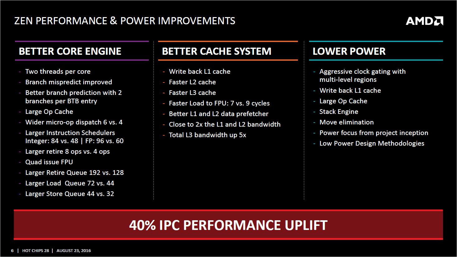
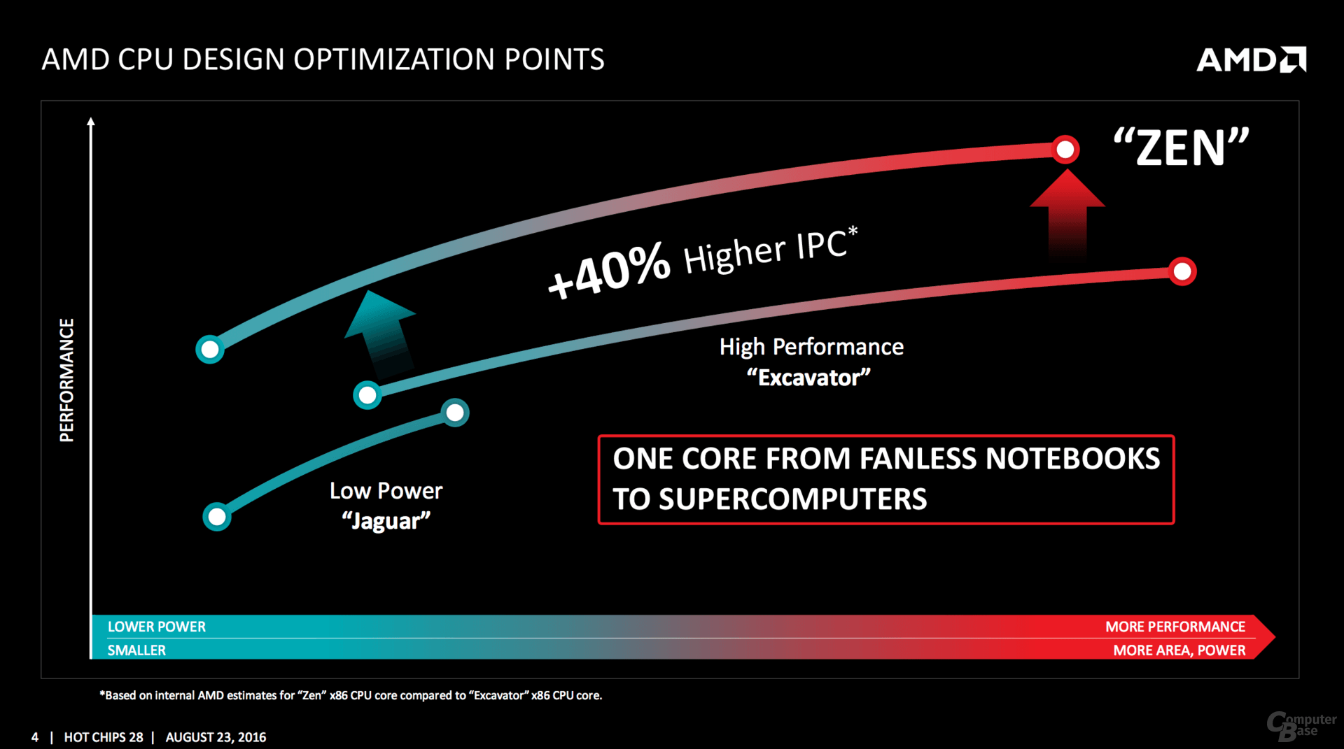
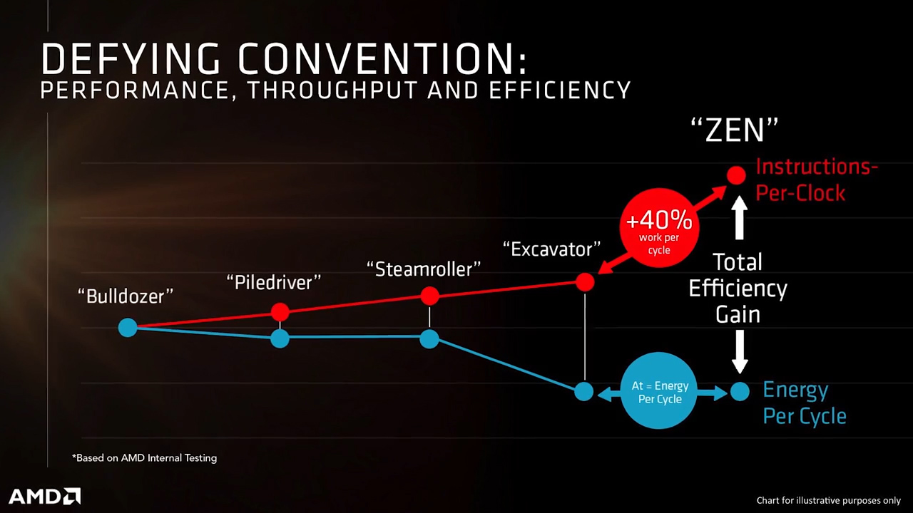
Right off the bat, AMD dedicate the first few slides of the Zen Hot Chips 28 presentation to reaffirming the improvements to Zen’s IPC (which is up 40% compared to the excavator architecture), energy efficiency and the cores scalability thanks to the Zen’s CPU clusters (we’ll get to that in a moment). AMD dedicate a slide to give a highlight reel of the various improvements to Zen’s architecture.
These improvements are separated into three sections- Better Core Engine, Better Cache System and finally Lower Power. The latter of the trio we discussed at some length in part one, so it’ll largely be ignored for this article. AMD are aiming to take a wider execution approach, leveraging better caching and prediction systems on the CPU, along with the SMT (Simultaneous Multi Threading) to keep the CPU as busy as possible and reduce stalls in the pipeline.
While the radical processor redesign is serving them well, the smaller node and FinFet process afforded to them with the 14nm FinFet from GloFlo must take much of the credit. We’ll leave talk of process refinements behind however, as we’ve discussed that at length in the previous part.
Modern graphics cards are built with scalability in mind – think of them as ‘lego pieces’, where a greater number of them can be plopped together to increase performance. CPU’s are being designed in this same, modular way, allowing the company to scale the number of processor cores easily for whatever task they’re designed for, and for a variety of price points.
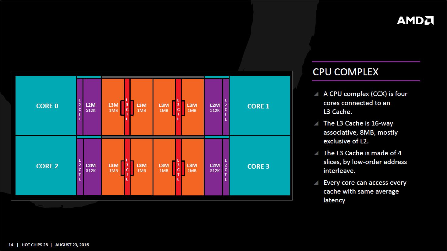
With this in mind, while it’s technically one of the latter slides of the press deck, I feel discussing Zen’s CPU Complex (known as a CCX) early on is imperative for having a good understanding of what AMD are trying to achieve with the upcoming CPU. I’m hoping that a basic understanding of what a CCX (CPU Complex) is, we can proceed throughout the rest of this analysis and separate the differences between the inner workings of a single Zen processor core, and the CPU as a whole.
Essentially, each of Zen’s CCX’s contains fours CPU cores, 8MB of Level 3 cache and 512KB of level 2 cache. This CCX approach allows AMD to tweak the processor for a number of SKU’s: for example, 8 cores, 6 cores, 8 cores – by simply ‘adding’ CCX’s together, or disabling a certain number of cores. This will likely be handy based on yields too – for example, in an instance where 2 CPU’s in a CCX are damaged, the the two CCX’s (one damaged, with only two cores working, the other fully functional) would result in a 6-core Zen solution, providing up to 12 threads.
There’s also the question of clock speeds of the different SKU’s; that is if the clock speeds of the 4, 6 or 8 core variants of Zen differ is currently unknown, and we currently only know that Zen’s clock speed is at least 3Ghz based upon the Engineering Sample tests.
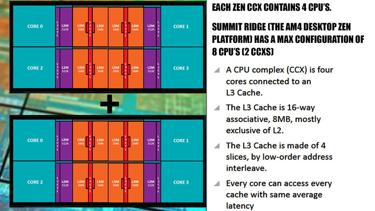
We’ll dig further into how Zen’s cache system works over the course of this very article, but for now, know that the Level 2 cache and Level 3 cache are mostly exclusive one one another, and this slide confirms an important factor – each of these four cores can indeed access the other cores Level 3 cache, but there’s a variable latency between this. For instance, Core 0 can access Core 2’s cache without any fuss (for sake of clarification, core counting starts at 0. So the first core is 0, core 3 would be the forth).
What is a Zen core? Certainly not a pile of secrets.
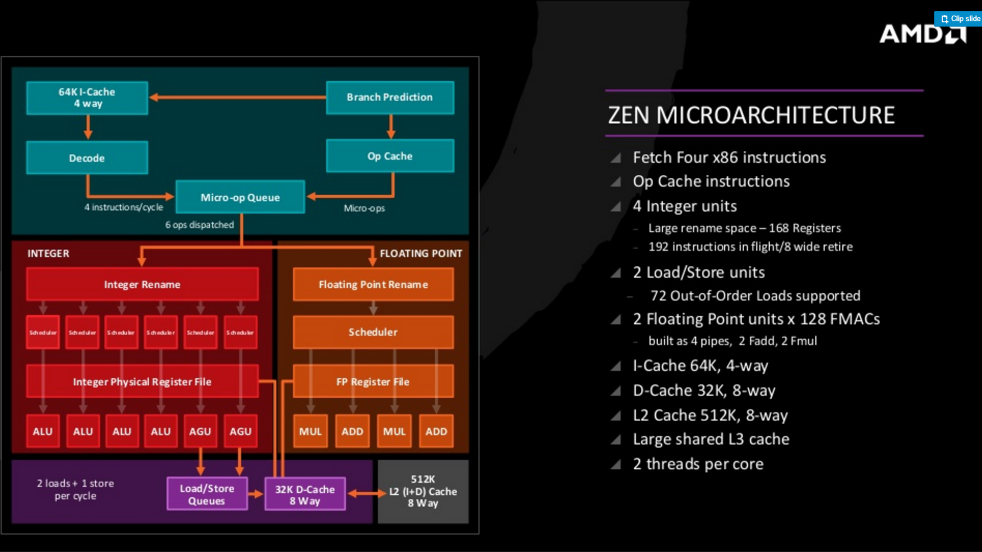
AMD have decided to rehash one of the Zen Microarchitecture diagrams, but have added additional info compared to the older slide. This updated slide provides a deeper look at the inner workings of a single Zen Core (remember, there are four Zen Cores which go into a single CCX).
Above, we’d touched on the Level 3 cache, which is indeed shared between other processors. As we highlighted in the first part of the Zen architecture analysis, AMD have separated the Integer and Floating point pipelines. The 4 Integer Units (INT) are coupled with a 160 entry register file (we’ll get to that), while the Floating Point contains a 160 entry register file (we’ll get to that too). The most obvious other featured touted (other than the caches, which we’ve touched on in part 1, but we’ll go into further detail in this article) is yet another mention of the SMT, which as we know allows a single Zen core to handle two threads simultaneously.
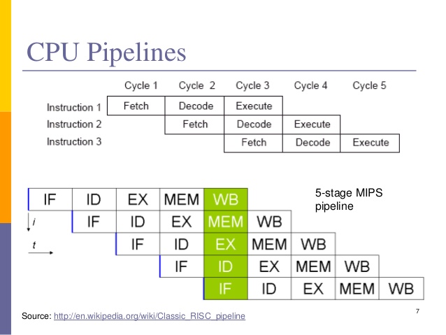
Processors work as a ‘pipeline’ which in essence fetches an instruction from the systems memory (the first stage), calculates that instruction and then sends that instruction back to computers main work memory or the CPU’s caches (the last stage), with multiple stages in between. For the purposes of this article, I’ll try to keep things as straight forward as possible to ensure everyone knows what’s what with the Zen specific information, but the larger subject of the CPU pipeline is outside the remit of this article, if you need a refresher I’d suggest checking out either the Instruction Pipelining article over at Wiki, or taking a peek at a pretty nice University paper on the subject.
Zen Fetches, it Decodes and it Executes with the best of them
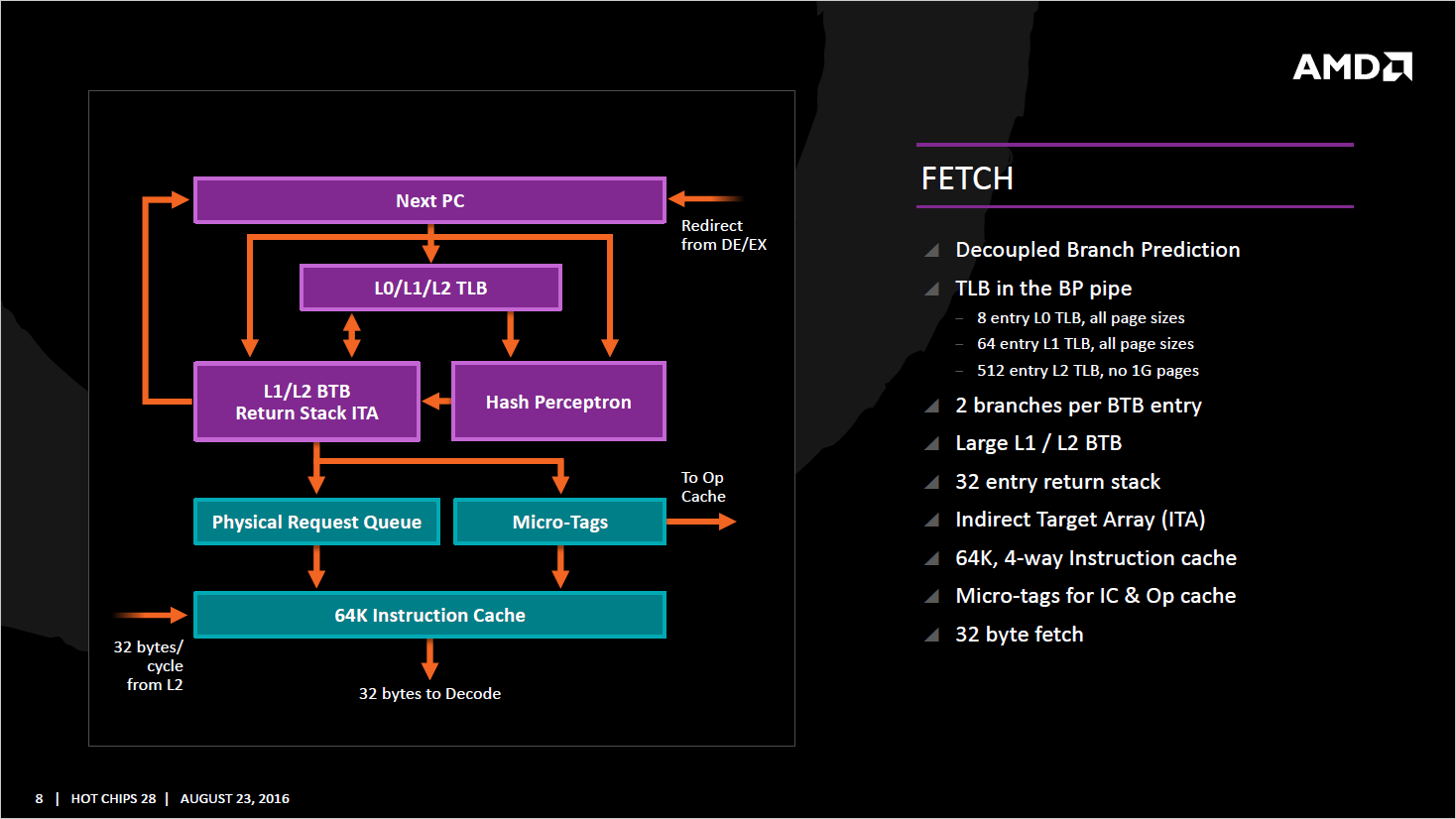
As mentioned above, Fetch is the first step in the basic CISC (Complex Instruction Set Computing… in other words, x86 CPUs) pipeline, and the simply has the CPU grab the relevant piece of data from whichever location it is being stored (contained in). In our previous part, we’d discussed how AMD were being very aggressive when it came to the improvements in Zen’s prediction, and here is a great example of that. Team green have opted to decouple the branch prediction. Branch Prediction simply is uses to ‘guess’ which direction a program will go in a structure using the traditional if – then – else structure, and by doing this, the pipeline will be better filled, because the CPU has the next instruction ready to go.
Because of the decoupled nature, the fetch has greater freedom to run ahead of the other components in the CPU, using some undisclosed internal algorithms for prediction . In theory; this will reduce the latency of the CPU and reduce pipeline stalls – but failure means additional energy is gobbled up.
AMD were less forthcoming on the size of the BTB (Branch Target Buffer) for Zen, with ‘large’ being the only information provided. Whether this is larger than the current (and soon to be older) architecture from AMD, Bulldozer, which for the sake of comparison is 512-entry, 4-way L1, with just a single cycle latency… well, we’ll have to wait and see.
The other key component to Fetch would be the Translation Lookaside Buffer (referred to as TLB), whose job is to reduce latency by keeping tabs on virtual memory and translate virtual memory addresses to a real, physical address (for more info click here). AMD list Zen’s TLB as Level 0 with 8 entries as any page size, Level 1 with 64 entries at any page size, Level 2 with 512 entries, but supports only 4K and 256K page sizes.
If you’re scratching your head throughout this information, just know that Zen will be efficient at fetching instructions from the computers memory, and (in theory) use less power while doing so. Really and truly, the purpose of all of this is to keep the pipeline as busy as possible, and this is imperative, because when the CPU is idle, you’re wasting processing time. Having idle cores or threads when the program is waiting for something to be calculated results in stalls, which in games for example, can lead to frame-rate hitches.
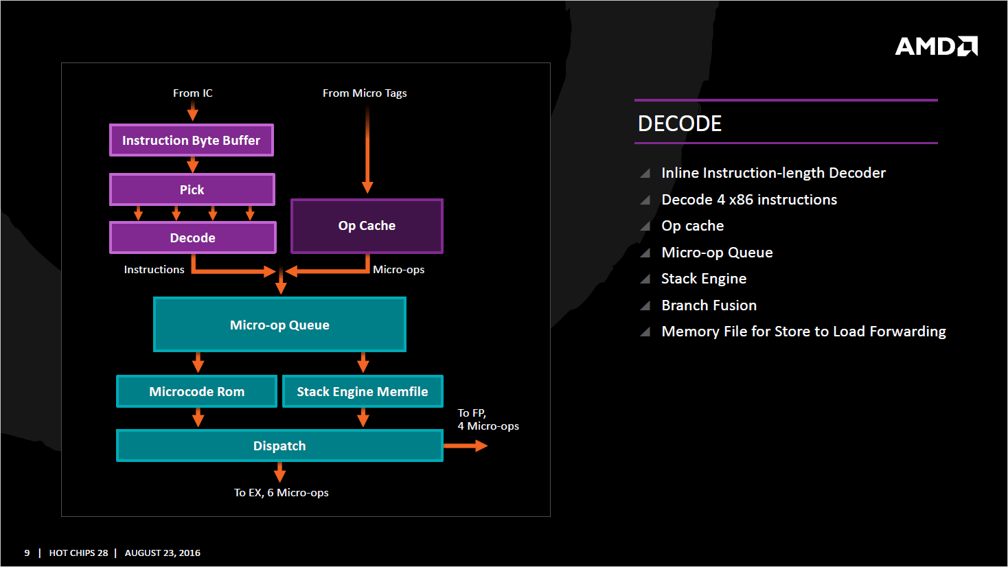
Next up is the Decoder, whose job is to “decode” the commands it’s received for the CPU specifically. You might be aware that various CPU’s have a variety of Instruction Sets, so once an instruction is decoded, it can then be executed by the relevant part of the processor core (we’ll get to that in a moment). AMD’s Zen core can decode four instructions x86 per cycle, which may be fused together, so that a micro-op (Micro Operations are low level instructions) will go through the micro-op queue (but still technically represent two instructions).
Zen also possesses a “Stack Engine” which is a new feature AMD added to the processor, and its function is to reduce power consumption of the processor. Taking place between the queue and dispatch, it uses already known memory addresses and saves the CPU from having to go through that entire step.
Finally, comes the dispatch from the Decoder, which sends instructions at either 6 per cycle to the INT (Integer) scheduler, or 4 per cycle to the Floating Point scheduler. Zen allows the dispatch unit to send off an instruction to both the Int and FP in the same cycle, and as one can imagine this increases the throughput and the processors efficiency considerably compared to the alternative approach, which would be for the CPU to alternate per cycle (for example, FP dispatch cycle 0, INT dispatch cycle 1, FP DIS Cycle 2…).
The next stage of the pipeline is Execute, and this is where commands (instructions) are actually carried out, and the result is then stored in a register. To put it another way, it’s the part of the CPU which takes the data and calculates the result of the equation it was sent.
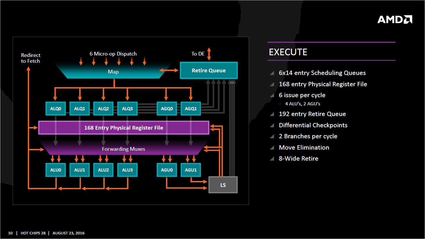
For Zen, the Micro-Operations (which we discussed a few paragraphs up) are now sent too one of two possible routes (which are located, once again, inside a single Zen core). The first is Integer (whole numbers… So for example, 1, 2 or 1024 are Ints) calculations, and the second would be Floating Point (which would be a number such as 6.349). It makes sense to start with the Integer first I suppose. There’s a 168-entry register (a register, to clarify, is a very fast storage location… so in this respect, the Int can store 168 ‘things’ here). and it sends that data into four ALU (Arithmetic Logic Units… the things which actually ‘do’ the calculation), and two address generation units.
As highlighted in the slide, this allows a single Zen core to schedule six Micro operations (per cycle) and execution port has its own 14-entry schedule queue. The Integer unit can handle two branches per cycle (also highlighted in the slide), but from what has been discussed during interviews, there are a few small limitations on this. The first is that the ALU’s are not equal in function – two are capable of branches, while only one can perform a signed multiply, while the final ALU handles CRC (Cyclic Redundancy Check) operations. From what AMD have mentioned, the ALU’s are all symmetric, but they do have some specialised operations – but the company are keeping rather tight lipped as to what these are for right now.
Zen’s Integer Pipeline will also keep tabs on the various instructions as they branch out. This serves two purposes – the first is it can nuke any data which happens to be the same result (basically saving storage space on the processor) and also uses what is known as Move Elimination. ME simply uses a ‘mov’ (Move) command if it needs to move that data from one register to another (say from reg 1 to reg 4). The CPU will then adjust the pointers to the new location (basically, the computer will now know that the instruction which was formally held in reg 1 is now in reg 4. Think of it as doing a find and replace in a word document on a word you made a typo on). The other ‘option’ for this would be to send the instruction all around the houses again, so this is a neater way of achieving the same end, being more efficient.
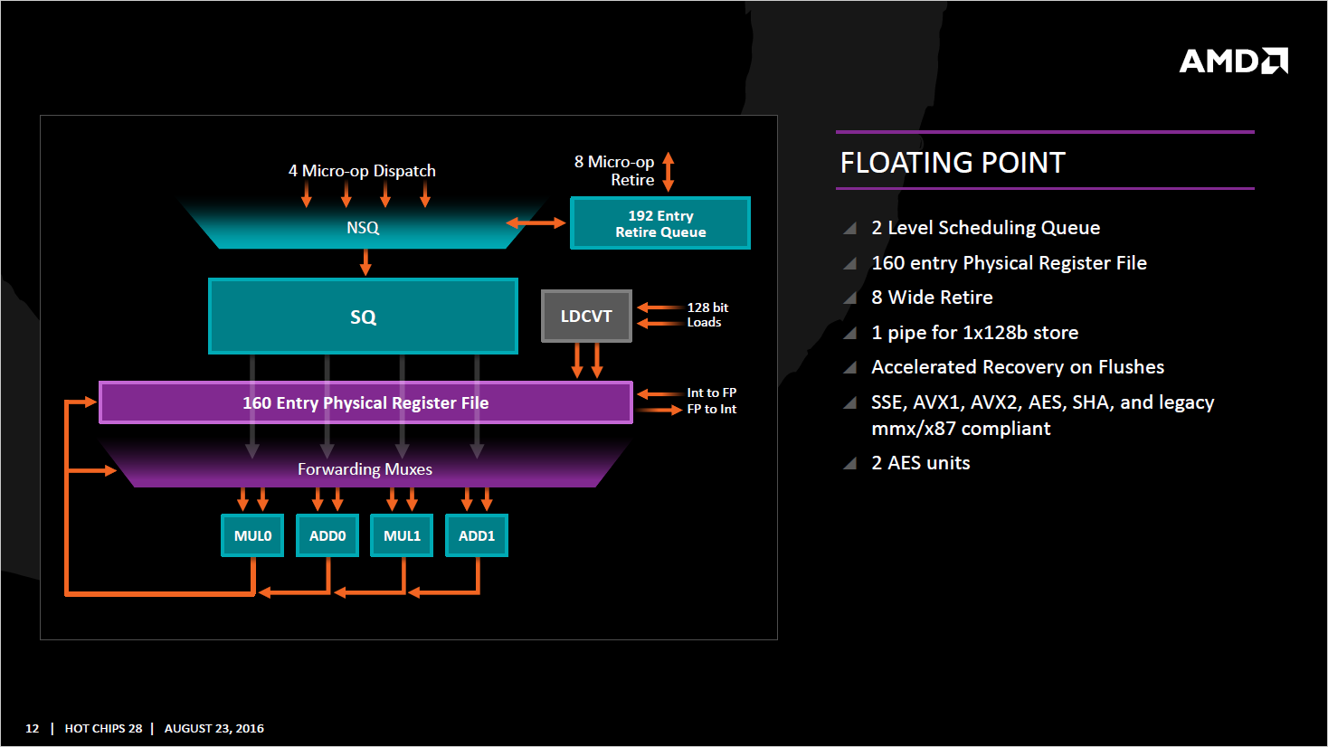
This brings us onto the Floating Point part of the core, which houses a 160 entry register file. As you can see in the diagram, if required, the floating point can be shuttled off to Int if required by the particular set of operations. AMD add a forth pipeline for the FP Unit over the Excavator architecture. AMD aren’t saying much about the latency of how all of this works, only that it is faster than the previous CPUs.
The Int and FP both access the retirement queue directly (just because an instruction has been ‘executed’ doesn’t automatically mean the result is back in RAM, instead it’s stored until ‘retirement’ , which is when the CPU writes back the data to RAM.). As you can see on the relevant slide, it’s 192-entry wide, and retires 8 instructions per CPU cycle. AMD aren’t skimping on the retirement portion of the processor, because just like the execution units being ‘starved’ of data because the CPU is fetching it too slowly, the reverse is also possible, and the CPU is being held up because data isn’t being pushed back from the processor to RAM quickly enough for the core to not be stalled and waiting.
Cache you later
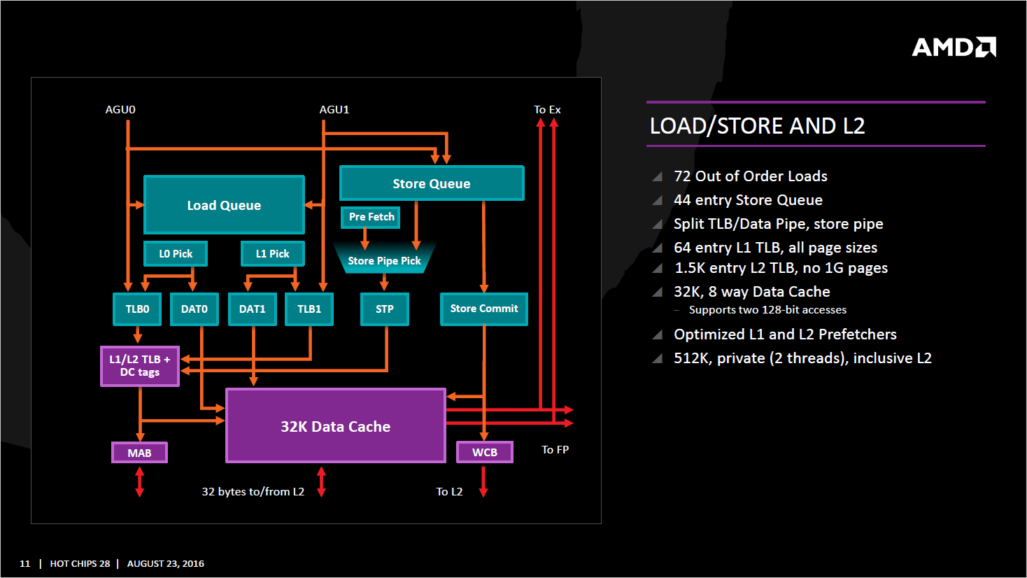
Now it’s time to learn about Zen’s Cache system, which other than being the basis of my immensely original (I’m sure no-one else has thought of such a clever pun) joke, it forms the backbone of the processors low latency access to data. Above we’ve discussed the that each Zen core has 512KB of its own ‘private’ cache, and also each CCX (CPU Complex) has its 8MB of level 3 cache. This level 3 cache works out to be 2MB per core, but each ‘core’ can access the others share of L3 cache.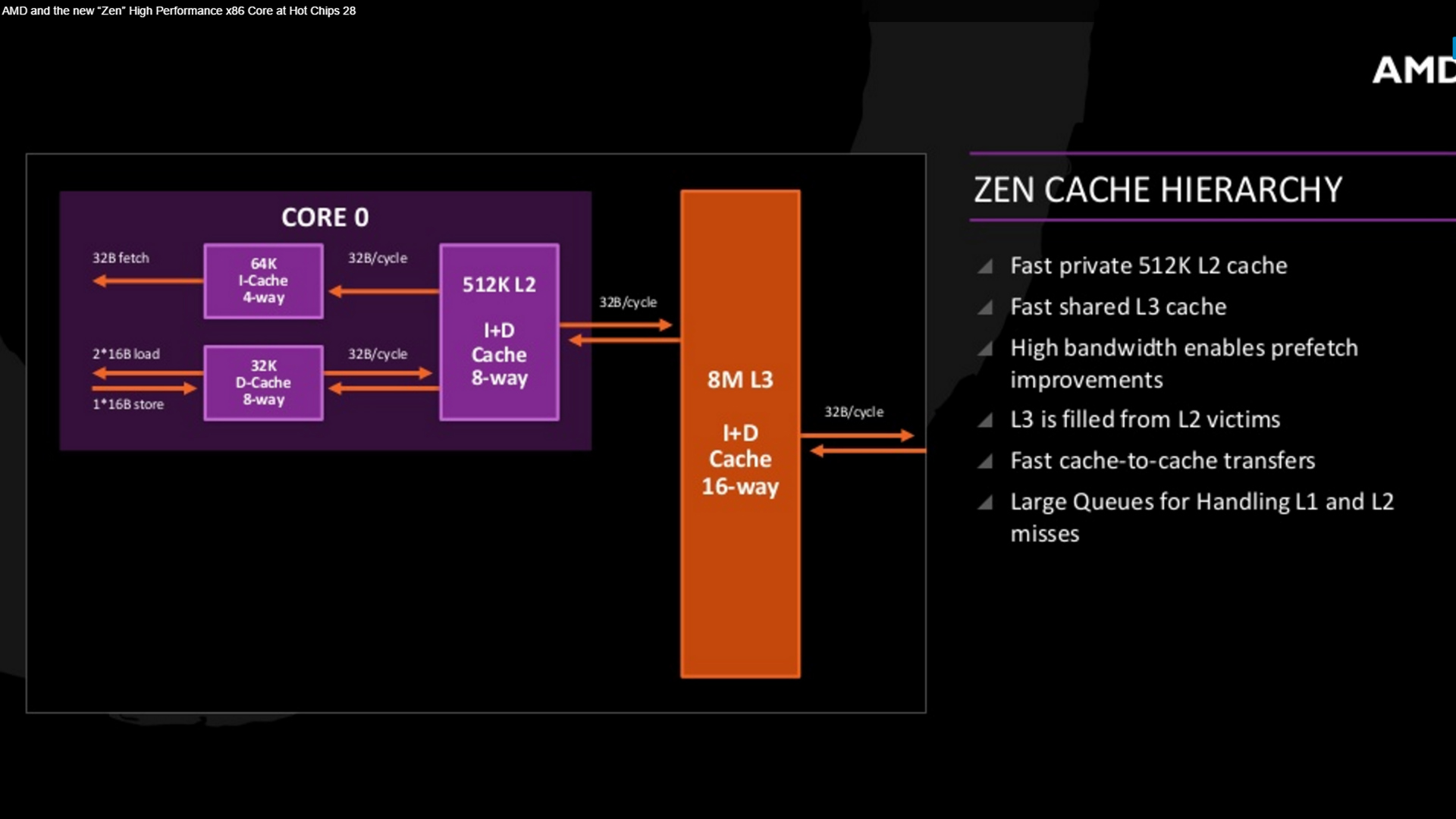
Level 3 Cache for Zen however is quite literally a Victim Cache, and this means that data that’s ejected from either L1 or L2 (due to that cache being required for something more pressing. Remember, L3 cache is slower than L2, which in turn is slower than L1. So data which is more frequently accessed or needed ‘soon’ is attempted to be kept in the fastest storage location possible). In theory, combined with the private 512KB cache per core, and because L3 is “mostly exclusive” of L2, duplication of data should be minimized, and thus more ‘stuff’ can be held.
If you’re familiar with Summit Ridge or benchmarks from AMD, you’ll be doubtlessly aware that there’s an 8-core Zen CPU, and this means that two CCX’s are in effect ‘joined together’. Logically, this means there’s a larger amount of L3 cache (16MB) shared between these 8 cores, but because the two clusters are ‘separate’ you might ask how the Core 0 (which, we’ll say is in CCX one) can access the level 3 cache which is in CCX two?
Well, as you can imagine, inter-chip communication is pretty important, due to memory controllers, PCIe, and also general ‘stuff’ to do with multi-threading. To this end, AMD are using a custom fabric which acts a a liaison between these clusters. Unfortunately, if you want more info on how all of this works… you’re somewhat out of luck, because AMD are remaining fairly tight lipped on the whole thing.
AMD Zen – Simultaneous Multi Threading (SMT)
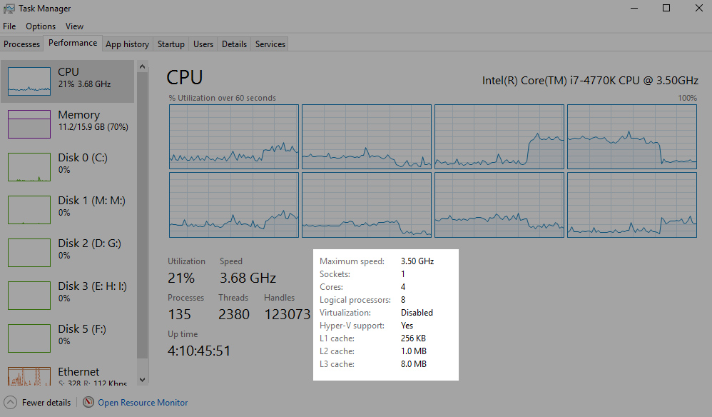
While the subject of threads in computing is quite complex (especially if we start going into Fibers) for the sake of this article, think as ‘threads’ as execution pipelines which can run different tasks. If you’re running Windows, you can load up Task Manager, and under the “Performance” tab, switch to CPU and checkout the number of sockets, cores and logical processors. Sockets quite literally represent the number of physical socketed CPU’s in the system, which will almost certainly read as “1” if you’re running a desktop PC, laptop or other similar device. Cores represents the number of physical CPU cores in the system, while Logical Processors are the number of threads possible to execute across all of those cores. So, for example on a I7-4770K from Intel, it has 4 physical cores, but due to HyperThreading, it supports 8 Logical Processors.
While Intel have certainly grabbed much of the public’s attention when it comes to SMT, there are a myriad of CPUs which use the technology… various IBM CPU’s do, and by extension the Xbox 360 (which has 3 cores, 6 threads) and the PS3 (1 core, 2 threads… plus a bunch of other processors on the Cell. For our analysis of the PS3’s Cell CPU click here).
Zen is AMD’s first foray into true SMT; that is – running more than one thread per CPU core, and the company have employed multiple technologies to ensure that pipeline stalls are minimized. This is one of the reasons AMD have pushed the branch prediction, cache and other assets of the Zen processor core so much above the older generation. Performance in an SMT core can be no greater (or, in some cases worse) than a regular core if it lacks execution resources which leads to stalls in the pipeline.
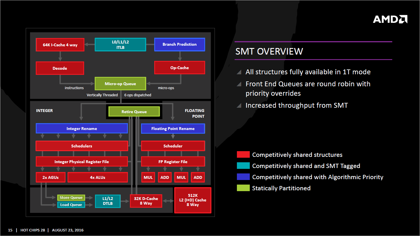
So, how are AMD dealing with ensuring that threads on the same core are handled correctly? Zen uses Round Robin, which in essence is a method of ensuring that tasks are given an equal time share, traditionally a ‘job’ will be interrupted even if it isn’t finished the time its ‘slice’ is up. So for example, if the core is processing two jobs (one on each thread), Job A gets half way done, is interrupted, Job B starts (and let’s say finishes, as it’s a shorter job) and then Job A continues.
But, you’ll notice at the end of the sentence AMD adds “with priority overrides”… so what gives? Well, Zen will run an analysis to see which threads require a higher priority, which will be based upon latency, stalls and quite simply if it’s more important. Think of it this way – sometimes, a job comes in that’s more important than the other job that needs to be done. It’s not that Job B isn’t important, or isn’t required to be processed, but Job A is needed ASAP, because it’s a key process and without it, the other threads from the application might be stalled.
With that said, you’ll notice there are four distinct labels in the above image, which means certain parts of the core are statically partitioned (so work is given even timing… in theory, this is likely for in-order operations, as in those cases, operation A needs to be completed before B, and will likely be primarily for the main processor Queues, such as Micro Operations or retirement).
The vast majority of Zen’s core is competitive however, which means that if a thread needs more time and love, the CPU will do its best to give that to the thread – assuming it’s able to achieve it that within that cycle, or it’ll have to wait until the next.
Zen’s Instructions – Something New and Something Old
While we’ve touched on what an Instruction is (and by extension, and Instruction Set) earlier in this article, I want to provide a bit of clarification. You might recall the steps above (simplified) were Fetch (grabbing the command from memory) followed by Decode, whose joy it was to translate it to an instruction that the processor can understand before it is sent off to be executed (in other words, that command to be carried out).
For the most part, x86 CPU’s (which Intel and AMD primarily focus their attentions) have a pretty compatible feature set – generally because the majority of those instructions are crucial for compatibility. The company have certainly had a few exclusives they’ve supported over the years (such as AMD’s 3DNow) but typically, the standards eventually cross over if they’re useful. If an instruction isn’t ‘built in’ to the processor, but the application requires it, then generally it will be emulated in software using an interpreter. This is a pretty complex subject, but basically it will use other processor functions to achieve a similar result to the originally intended instruction – albeit with a performance cost.
A few simple examples of what an Instruction Set might contain includes Add (which does exactly what you’d expect, adds two numbers together), Load (literally requests the information to be loaded from RAM to the CPU), Store (store’s that info to RAM) and In (input info from a peripheral, in other words accepting something from a keyboard).
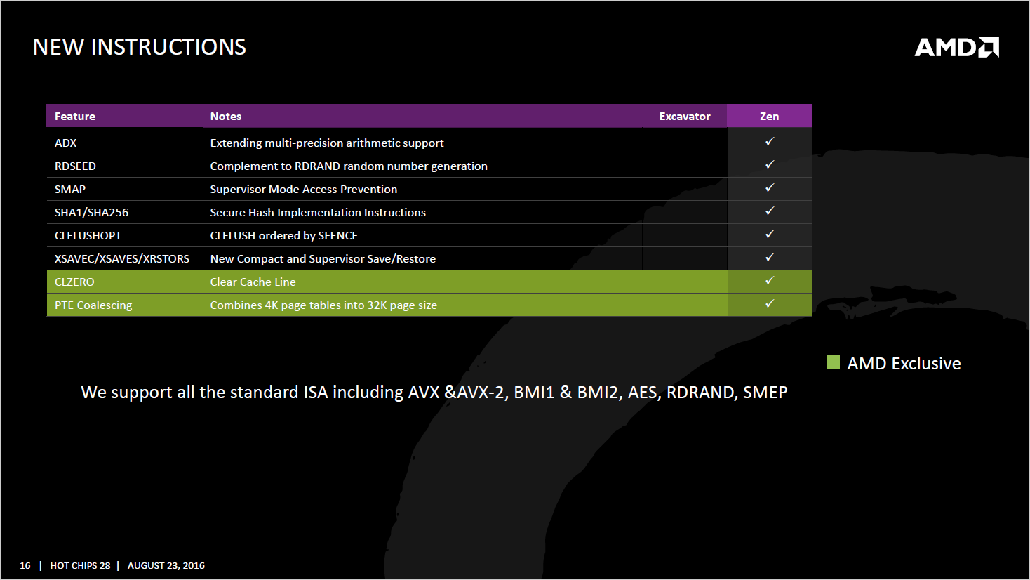
So now we’ve got the basics ‘out of the way’ let’s talk about Zen specifically. As you’re probably expecting by now, AMD are supporting the standard x86 ISA, adding a few new ones which Intel support currently, but AMD aren’t with their current architecture and new instructions which will be exclusive to Zen.
RDSEED is for random number generation, and a bunch of other stuff which is for either cryptography or other uses. The two new instructions for Zen / AMD specifically are CLZERO and PTE Coalescing.
The former (CLZERO) clears a specific cache line and will likely be rather exciting for High Performance Computing areas (which is one of the primary markets AMD are targeting…). The purpose is to quickly clear cache pollution, to simplify, cache pollution is unneeded data in the cache which has been loaded in and is clogging up that cache when it could be used for a relevant piece of data. So CLZERO from Zen will easily allow the cache to have an entire line cleared if needed. Because the cores handle multiple threads (SMT) and due to the cores themselves sharing L3 cache (or at least, can access the others cache) it’ll be useful across both L1 and L2 cache for a single core, and likely even more helpful for L3 Cache.
https://www.youtube.com/watch?v=Asdw2xTKh_g
PTE Coalescing (PTE stands for Page Table Entry) from what we understand allows 4K page tables to be combined into 32K page tables (a page table is used to map virtual addresses and physical addresses. Due to programs sometimes ‘paging out’ pieces of data into other secondary storage – in other words, Virtual Memory on the hard disk to save RAM, the CPU needs to keep track of this if / when the data is needed again). In theory (you’ll notice that disclaimer used a lot throughout this article…) it’ll reduce the usage of the TLB (Translation Lookaside Buffer… which stores recent translations from Virtual Memory to Physical). From what has been revealed, it’ll only work when specific criteria within the Branch Predictor are reached.
Zen’s Performance – Will It Really Beat Intel?
As I explored in the video below, there are still a number of questions raised regarding the performance of Zen – despite AMD showing off a benchmark clearly putting the 8 core / 16 thread Summit Ridge desktop part up against an Intel I7-6900K. With both CPU’s clocked at 3Ghz (due to Zen being an engineering sample), it pipped the I7-6900K from Intel to the post by about two seconds in Blender. It’s not really a major advantage – but that wasn’t the point of the demonstration, instead it was to show that AMD are ‘back’ to being competitive in the high performance stakes with one of Intel’s best.
https://www.youtube.com/watch?v=8pJJgV6kdG8
But with that said, as I covered (in detail) in the video, there’s a whole bunch of questions still to be raised regarding Zen’s performance in ‘the real world’. In a typical benchmarking scenario (the type we’d run if we were conducting an actual review of Zen or any other product) you’d naturally compare the part across several (relevant) applications. Blender (in this example) could be one application Zen is particularly strong in. Considering Blender is open source, it’s possible AMD tweaked the code a little to better use the new instructions Zen affords (for example), which could have just been enough to give the new processor the edge.
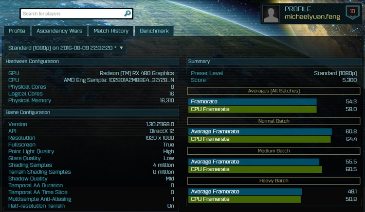
The only other benchmark we have, aside from the official AMD Blender benchmark (which once again pits the unnamed 8 core / 16 thread Summit Ridge CPU against an Intel Broadwell-E I7-6900K) are a few Ashes of the Singularity benches. Unfortunately, the benches don’t really reveal that much info on the performance, except that it’s roughly on par with other competing processors. These processors were two distinct revisions (if you read the serial numbers), but both had 8 cores, 16 threads and the GPU was an AMD Radeon RX 480.
Unfortunately, these AMD Zen Benchmarks aren’t particularly high on the trust scale, not because it’s questionable if they’re actually really Zen (that user has been seen with other AMD products previously), but because we don’t know the state of the Engineering Sample being tested. For all we know, some of the cache wasn’t functional, or had other defects on the core which hindered the performance, and possibly isn’t the same processor we saw fighting the Broadwell-E to the death.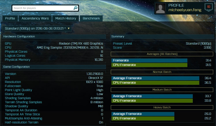
Then there’s the “how fast does it clock” question – and while I don’t like to harp on too much about clock speed (as different CPU architectures accomplish different workloads per cycle… like how Intel needed to crank the Pentium 4’s up to 2.5 to well over 3Ghz to compete with the Athlon’s which were running at the 1.7-2.4Ghz back in the day). But in this instance it’s incredibly relevant, since AMD are using the same clock speeds as the Broadwell-E as a point of comparison, therefore saying that two architectures (Zen and Broadwell-E) will be trading blows at the same clocks. So, given what we know about the Engineering Sample Zen – is 3Ghz a walk in the part for the retail Zen processors? It’s possible the CPU could be cranked all the way to 4.5 or even 5Ghz without effort, or will it struggle to turbo past 3.4Ghz?
In a similar question to the base clock speed, what’s the overclockability of Zen like? Will it be totally unlocked, and does it overclock well like certain Intel CPU’s, or will the silicone already be pretty close to the ceiling and therefore we can’t really get that much more out of it, other than say another 200Mhz on average?
Intel aren’t going to be sitting on their asses and waiting either – as right now Kaby Lake will be likely released for Desktops in the new year (Q1 2017), so we need to see what happens. Intel are promising about a 12 percent boost in performance over Skylake, but when you consider that the layout of the cores will be 4 cores, 8 threads… Zen could be an excellent buy, even if the per thread performance is a little lower.
But this naturally leads us to another key point – what’s the pricing going to be? Are we going to see the 8C / 16T Summit Ridge be sold for say the same price as the I7-6700K on release (about 330 – 350 pounds), or will it be more like 500? And what about other SKU’s in the lineup? Rumor has it AMD wish to focus on the higher core count of Zen first for Desktop, and then slowly release the 4 core models (so just a single CCX) or 6 core models later on… but we’ll need to wait on if that rumor is accurate!
With all of that said, Zen is looking to be an incredibly interesting processor. And it’s imperative to remember that AMD doesn’t need to ‘beat’ Intel at everything. They could be 5 percent slower but if you’re saving say 20 percent of your cash, for gaming in particular (where much of your FPS is based on the GPU rather than the CPU at higher resolution or details) and they’d still be incredibly popular for gamers.
For the future, we’ll see the Zen+ processors (which we presume will be released a year or two after the original architecture debuts), and we can assume we’ll see the usual 10 – 20 percent IPC improvements, and possibly a slight tweak to the feature set and clocks. Whether or not Zen+ will sit on the AM4 platform or not isn’t revealed. And naturally how it competes against Intel (once again) remains a bit of a mystery.
As usual, stick around with us and we’ll keep you up-to-date on all the news and analysis of Zen and other hardware!


