Robert Hallock, AMD’s Head of Global Technical Marketing was kind enough to agree to an interview to discuss several key upcoming technologies for gamer’s, including Vulkan, DirectX 12 and of course, High Bandwidth Memory (HBM).
This first of a two part interview will be focusing on AMD’s decision to provide the base for Vulkan and what HBM is and why it’s such an important next step from GDDR5 RAM, the memory traditionally found in today’s graphics cards.
RGT: Can you tell us why High Bandwidth Memory is so important for next generation GPUs / Processors, such as the Radeon 300 series?
RH: “It really comes down to three issues: performance, power and size. GDDR5 has been around for about seven years, and has been a wonderfully productive technology in that time, but it’s reaching a point in its life where each additional MBps of bandwidth consumes a disproportionate amount of power. That’s a poor equation for client devices (e.g. CPUs, GPUs, SoCs), where your fixed amount of power consumption has to be balanced between ASIC* and DRAM power.
“If you can’t afford enough wattage to the ASIC, because memory has started to consume too much of the total, then ASIC performance begins to fall off over time—nobody wants that! We can solve that with HBM. HBM resets the power/performance curve on DRAM by more than seven years, as it’s over 3.5X more power efficient than GDDR5.
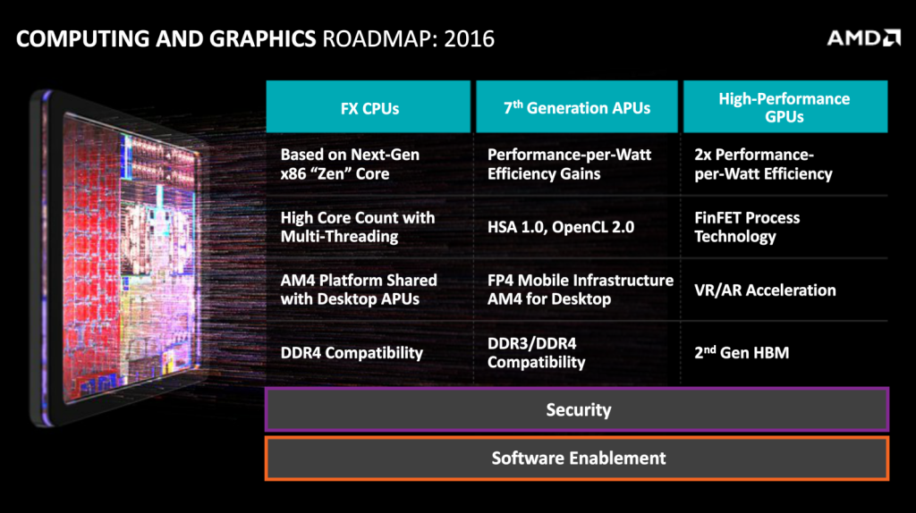
“I also mentioned performance. The direct outcome of a faster ASIC is a larger demand for more bandwidth from memory, and those demands will quickly exceed what GDDR5 is technologically capable of providing as ASIC generations progress. Computing is all about pushing back bottlenecks, and I think that HBM paves the way for much faster graphics engines that would otherwise be data-starved by GDDR5.
“Finally, form factors. People appreciate smaller devices, and a chief way to make a GPU smaller is to reduce PCB complexity. GDDR5 memory chips, traces and power circuitry consumes considerable area on the PCB. And your bus width is effectively determined by how many chips you have at 32-bits per chip. So if you make a board smaller or less complex by eliminating DRAM, you also sacrifice memory bandwidth. HBM solves that problem by collapsing all of the DRAM alongside the ASIC on a single svelte module called the “interposer,” and all of the area that GDDR5 used up is now freed up.”
*ASIC stands for Application Specific Integrated Circuit (pronounced A-sick), and is a custom designed chip for specific purposes.
To explain a few of the technical terms Robert brought (if you’re unsure), GPU’s have a certain amount of power they can draw and heat which can be dissipated by the cooler, and is the reason GPU’s sit at around the 300W max range. RAM requires power to operate, and this power eats into the total amount available to the GPU, and thus takes the maximum amount of power which could be routed to the actual graphics processor.
By reducing the power consumption of the RAM, a GPU vendor can save power and heat to channel into the GPU, allowing for a more powerful device. Or in the case of a low power system, uses less energy and becomes more efficient. While there are certainly other ways to reduce TDP (such as shrinking to a smaller process, say 20nm down to 16nm) it doesn’t solve the problem of memory power consumption, it just somewhat sidesteps the issue.
For a very simple and highly inaccurate (math wise example) say a Graphics Card is 300W, and the RAM eats up 100W – this leaves 200 available to the graphics processor on the card. If you reduce this number to say 50W, then the processor can be allocated that additional power (making it 250W). Once again these figures are not accurate in the slightest, and purely to help you visualize why HBM is important.
How did AMD become involved in the project for High Bandwidth Memory, and could you tell us of AMD’s role?
RH: “It’s a little-known fact that AMD is a huge player in the memory space. Joe Macri is Vice Chairman at Large on the JEDEC board of directors, for example. And AMD was behind the initial proposals for GDDR3, GDDR5 and now HBM. In a very real way, AMD engineering and proposals have set the tone for PC GPU memory for over a decade. In creating a technology like GDDR5, naturally we were also intimately familiar with its strength and weaknesses over the long term.
“As GDDR5 was entering the market on retail devices, we were already starting work on HBM as an eventual successor that would solve the long-term challenges and move the GPU industry another big step forward in the memory space. Seven years later: here we are with HBM!”
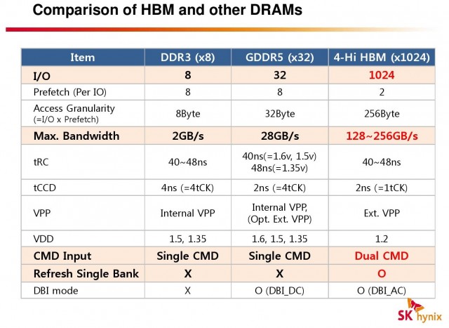
Is GDDR5 memory currently bottle-necking high end GPU’s, – for example the R9 290X, or is HBM more a preemptive, future-proofing measure?
RH: “There are certainly applications out there that specifically benefit from greater memory bandwidth, especially fillrate limited scenarios. But performance scaling across resolutions also benefits from greater memory bandwidth, and as 4K/5K res come onto the scene in force, that scaling becomes more and more important.”
HBM doesn’t rely on extremely high clock speeds (like GDDR5) and instead, relies specifically on an ultra wide bus (1024 bit) to provide it’s additional performance. Could you elaborate as to the reasons behind this?
RH: “High clockspeeds aren’t bad, but they’re also not explicitly good. High-frequency GDDR5 has taken the graphics industry to 320GB/s+ in an age where it was needed, but high frequency costs power, and high frequency also costs complexity. It takes more silicon and electrical devices to build memory controllers and power circuitry that can reliably sustain the higher clockspeed. GDDR5’s high clockspeed is a virtue of the per-package pincount, where each GDDR5 chip only offers 32 bits of bandwidth. So you have to gang lots of chips together, then run them at high-frequency QDR signalling to reach an appreciable bandwidth figure.
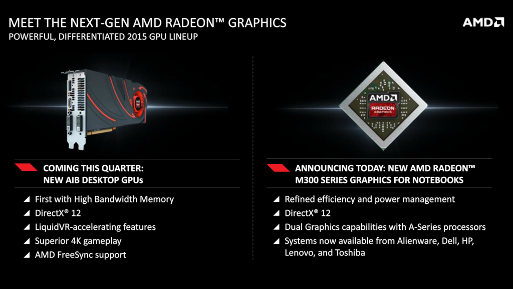
“If you can build a technology that runs at a lower clockspeed, and do so without sacrifice, then you definitely want to do so. Our solution to that want is the high-speed manufacturable interposer. The interposer is something of a silicon motherboard, through which we route incredibly dense traces [think wires – editor] — trace density that couldn’t be done on a normal PCB. And with that density you can put down a stack of HBM that offers a 1024-bit memory interface. You can use multiple stacks, each with a 1024-bit memory interface. Because your bus width is now so wide, you can afford to run at a much lower and more power-efficient frequency. You can also use tried-and-true DDR clocking, which reduces complexity all throughout the product. Overall it’s very advantageous for HBM to run at the low frequencies it does.”
As an editors note – bus width is increase with GDDR5 by stacking multiple chips on the PCB of the video card, and depending on the width of the bus, more chips are required. As Robert points out, GDDR5 is only 32-bit in width, and so to have a meaningfully ‘wide’ bus (say 256-bit, 384 or even 512) eight or more chips must be placed on the PCB. Having a total of 16 on a PCB side takes up a huge amount of space, and as Robert said, means you’ve got to have a lot of supporting ‘parts’ to regulate voltage and route data across the board.
In one of your press slides, you’d mentioned developing a high volume interposer solution, which the stacked HBM and the GPU (or other processor) sit on. Could you explain a little of what an interposer is and what challenges it provided?
RH: “I touched on the interposer pretty heavily in my previous answer, but it’s worth pointing out that the interposer is not a new idea. But what is new, what AMD did invent, is an interposer suitable for a high-performance ASIC. Past designs from other companies have been for small devices like FPGAs.
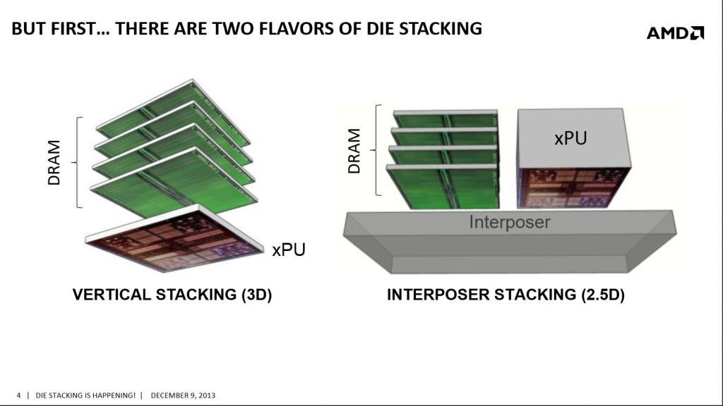
“The interposer isn’t the challenge, though, it’s the solution. There is a tremendous need and desire to integrate disparate functions into one discrete chip or package. Over time we’ve seen the trend: northbridges, southbridges, graphics, PCI Express, voltage regulation, caches… all of this has been brought into the processor over time. Why? Because it benefits power/size/performance, the holy trifecta. DRAM could definitely use the benefits of integration, too, but the processes used to make DRAM are not compatible with the manufacturing processes used to magic logic chips like SoCs or GPUs. So if you cannot integrate in the way people expect (e.g. “on-die”), then you find another way to integrate: the interposer.
“The interposer allows for the integration of very different logic and DRAM processes with on-chip power/size/performance benefits. You can use the right manufacturing techniques or node for each type of component, then stick it together like LEGO.”

Because of the lower power requirements for HBM, is it fair to say that it will work extremely well in a wide range of devices, including low power devices such as ultra thin laptops?
RH: “While we have not announced any specific plans, HBM could indeed apply across our product portfolio. HBM is of great help to any device that could use a better balance between ASIC power, DRAM power and bandwidth at a given wattage.”
For a modern GPU, such as the R9 290X how much power is consumed on GDDR5, and how much will be saved switching to HBM?
RH: “We’re not yet ready to talk about specific wattage, but HBM uses over 50% less power.”
Can you give any insight into how long AMD and its partners have been working on High Bandwidth Memory?
RH: “The initial proposals from AMD were written about 7 years ago, now.”
It’s my understanding that AMD provided a lot of code from Mantle towards Vulkan and some in the tech industry dub it Mantle 2.0. Why did AMD decide to push so much of its code towards the project?
RH: “Mantle changed the world. Game developers were in great need of a PC graphics API that achieved better control and better hardware performance than what was available. Developers saw how much work they could do per TFLOP on the console, which have always had LL-APIs [Low Level APIs – editor], and greatly desired something like that on the PC. They went around to every GPU vendor, but AMD answered the call and delivered the solution—Mantle—many months ahead of anything like it. Mantle was in development and launched for over three years before another contemporary appeared.
It had been a stated goal of ours to transform Mantle into an industry standard, or spawn a set of standards that behaved like Mantle. With our contribution of Mantle to the Khronos Group, we achieved both goals. Now, Vulkan certainly builds on Mantle and extends it to hardware and operating systems that Mantle never supported. The Khronos Group has worked very hard to make Vulkan a uniquely powerful API, and AMD cannot take credit for what has been done there beyond our contribution to jumpstart the effort. But we are proud that they saw the value of our work and agreed that Mantle was the right foundation.
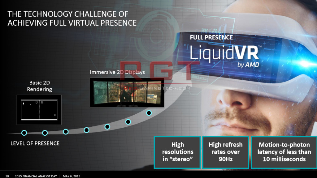
“Despite inaccurate reports to the contrary, Mantle also lives on and is evolving as a standalone API. For example, it’s the hidden nucleus of our LiquidVR project. Fast, responsive and interoperable virtual reality is the new frontier of our industry, just as the draw call was in 2013/2014, and we’re putting significant effort behind establishing ourselves as the go-to platform for VR in both hard- and software. We are also continuing our discussions with multiple vendors on utilizing Mantle as an innovation platform for select partners with custom needs, though I can’t say much more than that at this time.”
For more information on Vulkan, you can take a peak at our Vulkan Analysis here.
Could you discuss your plans for True Audio and TressFX, will you continue to push the technology? TressFX 2.0 saved a lot of GPU performance, correct?
RH: “TressFX 2.0 [see our TressFX 2.0 analysis here – Editor] was a huge step forward in performance and quality. We added:
· new support for grass and fur;
· continuous LODs for performance scaling with distance from the player’s POV;
· improved performance with many light sources;
· self-shadowing for texture and depth;
· modular and open code with porting documentation;
· and some tweaks to the physics model to make it more reliably lifelike.
“We’re on the verge of TressFX 3.0’s arrival. It’s incorporated in the Dawn Engine powering Deus Ex: Mankind Divided, the upcoming DirectX 12-ready game we’re working on with Eidos Montreal. TressFX 3.0 brings improvements to collisions, shape preservation, stretchiness, wind effects, anti-aliasing and translucency.
“AMD TrueAudio is particularly salient in this new world of virtual reality, where three-dimensional auditory cues must align with three-dimensional visual cues. It’s very disorienting if these two senses are mismatched, and AMD alone offers the hardware/software solutions to unite the two at high speed and with high quality. That’s all I can say for now!
“Thanks for giving me the chance to talk about these technologies. :)” – Robert Hallock, AMD’s Head of Global Technical Marketing.
Thanks once again go out to Robert and AMD for agreeing to the interview, stay tuned for part two and for further coverage of AMD’s products!
[schema type=”product” url=”https://redgamingtech.com” name=”AMD Interview with Robert Hallock on High Bandwidth Memory & Vulkan” description=”An exclusive interview with AMD’s Robert Hallock, discussing High Bandwidth Memory, Vulkan, TressFX 3.0, Liquid VR and other upcoming GPU technologies.” brand=”AMD Radeon” manfu=”AMD” ]


